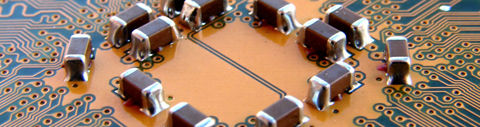
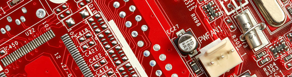
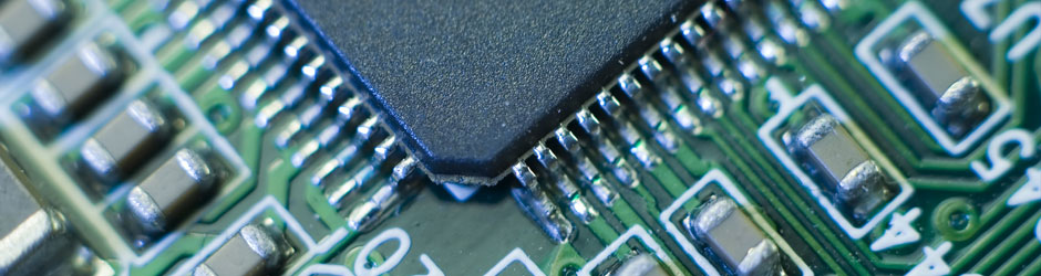
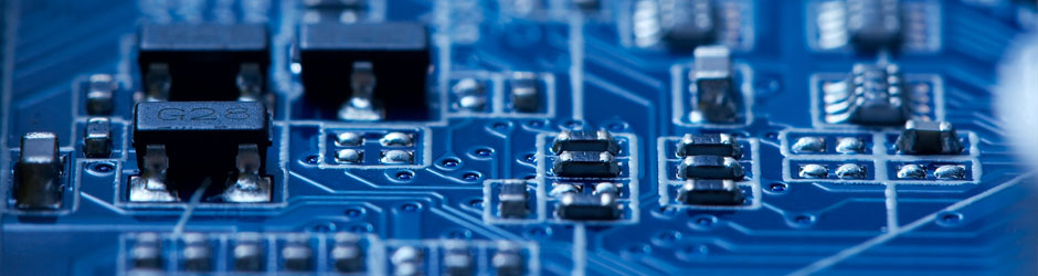
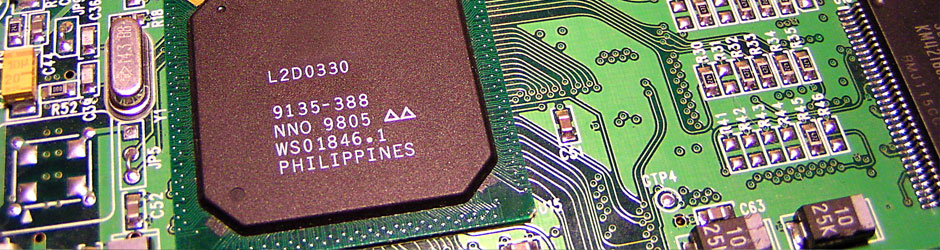
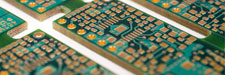
We have complete in-house assembly capabilities to provide a full turnkey solution to our customer’s needs. We assemble all variations from basic thru hole to very fine pitch Micro-Ball Grid Arrays (BGA), servicing industries from Aerospace and Government to Commercial including telecom, computer, peripheral, and multimedia industries.
Whether you have one circuit board or a thousand, Hughes can expedite your project. Rely on Hughes for maintaining complete control of both fabrication and assembly.
We understand that a seamless time-to-market is critical and time-sensitive for your applications. And as a result, our customer base is expanding because of their frustrations with other manufacturers. Hughes Circuits is committed to providing our customers with high-quality printed circuits and assemblies with superior engineering support. We know our success depends upon yours!
Click here to submit a quote request
General
|
SMT Automated Machine Placement
|
PCB
|
Thru Hole
Solder Chemistry
|
Rework
|
Inspection
|
Click here to submit a quote request
 Our Advanced Microelectronics group now offers advanced microelectronics assembly and packaging services, process development, and low to medium-volume production for high-reliability applications. Utilizing our new state-of-the-art equipment and our 45+ years of process expertise, we enable customers to transition from prototype to low-volume production seamlessly.
Services to meet your advanced assembly and packaging needs:
|
|
 Access to advanced packaging as a service, with no long-term commitments. This allows companies to conduct low-risk experiments, process development, and accelerate the time to market without having to purchase expensive capital equipment.
|
|
Click here to submit a quote request
| EQUIPMENT | SPECIFICATION | CAPABILITY |
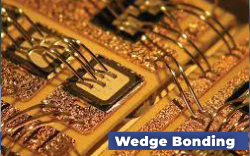
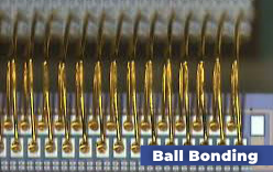
| TPT HB-16 Wire Bonder |
0.7 mil to 3.0 mil (17-75um) round wire (wedge or ball) |
Gold and Aluminum Wedge Bonding as well as Gold Ball Bonding and Bumping |
| Tresky T-5300 Die Bonder | 1um placement accuracy (application dependent) 20g to 4kg bond force |
3D packaging of MEMS, VCSEL, Photonics, etc. Epoxy or eutectic die attach Flip-chip attach Epoxy dispense or pin transfer |
| Keyence VHX 7000N Digital Microscope | 20x to 2,000x zoom optics +/- 60 degree viewing angle Coaxial, Oblique, and back-lit illumination Depth composition Image stitching |
Sub-micron resolution images |
| XYZTEC Condor Sigma Pull/Shear Tester | Tests from 1 gram to 200 kg force 24-bit resolution 6 Sensors in Rotating Turret |
Fine Wire Pull Test (Destructive and Non-Destructive). Ribbon Pull Test (Destructive and Non-Destructive). Die Shear Test Automatic Testing Capable |
Click here to submit a quote request
search terms:
HCI offers a complete design service including Schematic Capture, Part Library work, Layout, Documentation, Conversions, Reverse Engineering, and Revisions.
We Use the Following Tools:
![]()
![]()
![]()
![]()
Hughes Circuits PCB Layout Design Group is a lean, fast-moving team that can respond dynamically to our customer’s needs. We work efficiently to produce extremely high-quality designs in a minimum amount of time. Our Layout Designers take an engineering-minded approach to layout, meaning that we pay attention to the functionality of each circuit to address the critical design points. We don’t just connect the dots - we leverage the information in datasheets and application notes to create practical designs that perform as required.
We take a modern approach to a timeworn trade. We know the value of tried and true practices, but the way things were done more than 10 years ago is not always the most efficient. PCB layout techniques and tools have been advancing at a rapid rate in order to keep up with the hardware that engineers and designers are creating. So, it is important to stay on top of the latest advancements in layout software, without getting distracted by shiny new features. We determine the most accurate, and efficient ways to complete our customer’s layout designs by leveraging both proven, and cutting-edge techniques. For example, we always use online design rule checking, and interactive routing to be quick and precise. But, we also know when to take advantage of auto-routers to reduce design time without sacrificing quality or confidence in the layout.
We commit ourselves to accuracy in all stages of the layout process, not just component placement and routing. Accurate component land patterns are the foundation for a well-done PCB layout. One wrong land pattern can scrap an entire manufacturing run, and it is hard to find these errors until it’s too late. That is why Hughes Circuits’ Layout team implements a peer-checking system for all land patterns we design. Every land pattern is looked at by two sets of eyes in an effort to eliminate all errors. We rely on IPC land pattern guidelines and naming conventions, as well as our own proprietary processes and automation, to quickly perform these checks. By investing 1-2 extra hours of time early in the design process, we can save our customers thousands of dollars in potential revisions.
Hughes Circuits’ Designers are well-versed in all of the 3 major ECAD platforms. This allows us to provide layout support directly in our customer’s native tools, rather than translating between software platforms. All Designers have completed IPC certification courses to achieve CID or CID+ status (CID – Certified Interconnect Designer). Our layout team has a broad range of experience in the electronics industry. We draw upon this hardware, software, and manufacturing experience to avoid pitfalls and overcome challenges in our Customer’s PCB Layout projects. Hands-on experience in the lab has provided our Designers with an end-user perspective that enables us to make good layout decisions for our prototype customers.
Our layout team is experienced in a broad range of board types and circuit types. We do everything from high-speed digital and digital-RF (audio/video/memory) to sensitive analog circuits (sensors, amplifiers), to high voltage/current power boards (transportation, commercial UPS products), to microwave substrates, to probe cards, to interposers and flip-chip laminates. In all of these categories, we do layouts for production products as well as first-stage prototypes. We are experienced in implementing features like ICT testability, commercial/medical safety, as well as requirements for aerospace/military applications.
Capabilities:
|
Delivery:
|
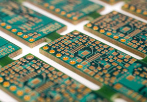 Hughes Circuits Inc. (HCI) has a complete bare board fabrication facility with all manufacturing processes in-house. When you place an order with HCI, you’re dealing directly with the manufacturer, not a middle man. Our domestic production is focused on advanced technology, high quality, and time-critical delivery while providing exceptional value. We provide extremely compressed lead times as well as right the first time engineering support. We don’t compete on bottom-line unit price, but we’ll exceed any other manufacturer in terms of the total value. Where price is paramount, we have partnered with quality off-shore vendors, so our customers can focus on their product development, not complex oversea supplier management.
HCI offers a wide variety of technologies, materials, lead times, and processes. Board types include standard rigid, high density rigid, chip carriers, high speed/RF, flexible & rigid-flex, thermal management, prototype, and highly engineered. We also provide extensive engineering support for materials, impedance stack-ups, surface finishes, leading-edge technologies, manufacturing guidelines, and general applications support.
We tool over 250 unique part numbers per month and more than 30% of our orders are shipped in less than 5 days. We also build mission-critical space and military electronics from 1 to 10,000, with each part ready for long-term reliability in harsh environments. We service an incredibly diverse customer base of over 1,000 customers, none of which comprise more than 10% of our revenue.
OUTSIDE THE BOX
We have three simultaneous operating environments, one built for high reliability, one built for speed, and one build for efficiency. we can build your mission-critical product using our conservative high-reliability processing guidelines. We can build multilayer’s reliably in 24 hours using our speed optimized production flow, or we can build your low volume commercial application inexpensively using our efficiency optimized production flow. If the price is paramount, we have partner offshore production facilities to ensure maximum price competitiveness.
- Our “FASTrack” system organizes the manufacturing process in to flow optimized “cells” which allow the product to move expeditiously limiting the amount of que waiting time before the next operation. This method is preferred for product lead times of less than 5 days on the standard product and less than 15 days on highly engineered products.
- Our standard manufacturing process is optimized to gain the highest level of efficiency to reduce manufacturing costs. This method is preferred for product lead times in excess of 5 days on standard technology and in excess of 20 days on highly engineered products.
- High Reliability, speed, or cost? Whichever you need, we’ve engineered the optimal process to ensure you’re on time and on budget.
- HCI is a woman-owned small business, AS9100D certified, MIL 55110 and MIL PRF 31032 certified, ITAR registered, and UL recognized.
- Experienced leadership and leading-edge manufacturing processes result in high-quality circuit boards. HCI has long focused on technologically demanding circuit boards, which has resulted in process refinement, equipment investment, and best practices training resulting in efficient and effective manufacturing for both simple and complex boards.
- Quality is built-in with HCI. All manufacturing processes are documented in our ISO9001 certified quality system. All quality inspectors are IPC 600 certified by our in-house certified trainer. HCI is qualified to build IPC 6012 class 3 as well as MIL-PRF 55110 and/or 31032 printed circuit boards. Every inner layer is inspected using the latest AOI technology capable of effectively inspecting .002” lines and spaces as referenced by the electronic CAD data. All boards are netlist checked before release to ensure the Gerber files as received match our production files and again at electrical test.
 |
 |
 |
TYPES OF BOARDS |
CAPABILITIES |
SERVICE AND SUPPORT |
|
HCI is part of a select few printed circuit board manufacturers in the united states with the capabilities to build almost any printed circuit imagined. For a complete list of our capabilities, please consult our FAB Capabilities page. |
|
Equipment Article Count: 4
Through investment in the latest technology software and equipment we are able to reduce cycle time, increase yields, and build higher technology product at competitive prices. Below is an outline of some of the equipment and technology that has made Hughes Circuits a service and technology leader.
Equipment Specifics Article Count: 3
Below are a few facts & overviews about some of the specific equipment that we use.
Equipment lists by division: Layout - Fabrication - Metal Fabrication - Assembly